Category:Semiconductor physics
Jump to navigation
Jump to search
study of semiconductors | |||||
| Upload media | |||||
| Instance of | |||||
|---|---|---|---|---|---|
| Part of | |||||
| |||||
Subcategories
This category has the following 9 subcategories, out of 9 total.
D
- Depletion region (12 F)
E
K
- Gennady Krasnikov (7 F)
M
P
Q
- Quantum cascade lasers (8 F)
S
- Silicon on insulator (6 F)
Media in category "Semiconductor physics"
The following 64 files are in this category, out of 64 total.
-
 27йцукеннн.JPG 549 × 500; 18 KB
-
 B-d-diagramsurfaceenergy.png 2,477 × 2,114; 324 KB
-
 B-e-phasediagram.png 1,811 × 1,471; 83 KB
-
 Bereiche der Leitungsmechanismen im Halbleiter DE.svg 575 × 450; 18 KB
-
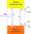
 Bändermodel Anregung.png 2,602 × 849; 65 KB
-
 Charge carriers concentration.png 564 × 84; 4 KB
-
 Ctlm rings.png 190 × 190; 8 KB
-
 Deep and Shallow SR profiles.jpg 3,600 × 1,912; 245 KB
-
 Delocalizacion de electrones en polimeros.png 1,011 × 328; 6 KB
-
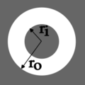
 Depletion width-en.svg 741 × 581; 4 KB
-
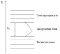
 Depletion width-ru.svg 741 × 581; 4 KB
-
 Depletion width.png 1,201 × 900; 42 KB
-
 Diffusion center.gif 473 × 356; 113 KB
-
 DOS.png 665 × 235; 4 KB
-
 Eigenleitungsdichte Si.png 661 × 624; 42 KB
-
 Electric potential.pdf 1,058 × 787; 36 KB
-
 Electric potential.png 1,000 × 700; 27 KB
-
 Electron Transport under Multiple Trapping and Release.png 3,997 × 2,294; 144 KB
-
 ExampleOfBulkPhotovoltaicEffect.svg 783 × 295; 28 KB
-
 Fig3DefectScattering.JPG 590 × 903; 31 KB
-
 Figure 9. The tribovoltaic effect at the liquid-semiconductor interface(136).jpg 1,385 × 1,675; 195 KB
-
 Hans-JoachimQueisser1995.jpg 1,429 × 2,321; 2.1 MB
-
 Haynes-Shockley experiment curve RUS.png 896 × 736; 62 KB
-
 Haynes-Shockley experiment ENG.png 1,013 × 474; 35 KB
-
 Haynes-Shockley experiment RUS.png 1,140 × 530; 42 KB
-
 Hiroshi Amano.jpg 1,024 × 683; 65 KB
-
 Hs1.gif 540 × 381; 6 KB
-
 ImpactIonisation1.svg 860 × 465; 34 KB
-
 ImpactIonization.PNG 321 × 471; 15 KB
-
 Inter vs intrasubband.svg 620 × 429; 13 KB
-
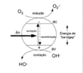
 Meccanismo fotocatalisi.jpg 1,280 × 720; 66 KB
-
 Mott-Schottky plot scheme.tif 1,313 × 2,082; 2.07 MB
-
 Mott-Scottky plot related to semiconductor-electrolyte junction.tif 1,313 × 2,082; 2.07 MB
-
 PDanim.gif 560 × 420; 352 KB
-
 Photoconductance decay measurement.svg 732 × 512; 17 KB
-
 Richard Swann glow discharge photo 1.jpg 247 × 238; 18 KB
-
 Richard Swann glow discharge photo 2.jpg 194 × 302; 17 KB
-
 Richard Swann glow discharge photo 3.jpg 210 × 201; 14 KB
-
 Schema 2D photomultiplicateur.jpg 840 × 556; 56 KB
-
 Schema effet photorefractif.png 851 × 400; 129 KB
-
 Semicond relation mu.png 557 × 169; 7 KB
-
 Semiconductor band-bending(español).png 667 × 512; 38 KB
-
 Semiconductor band-bending-en.svg 723 × 524; 2 KB
-
 Semiconductor band-bending-ru.svg 723 × 524; 2 KB
-
 Semiconductor band-bending.png 667 × 512; 37 KB
-
 Semiconductors (5884868648).jpg 501 × 500; 325 KB
-
 Semiconductors, selective behavior (5884302541).jpg 2,232 × 1,875; 1 MB
-
 Semiconductors, selective behavior (5884302787).jpg 2,232 × 1,875; 979 KB
-
 Shockley-Read-Hall model inorganic semiconductors.png 181 × 156; 1 KB
-
 Spvapparatus.png 844 × 420; 23 KB
-
 Stark-exp.jpg 1,755 × 1,240; 633 KB
-
 Stark-sim.jpg 1,755 × 1,240; 620 KB
-
 Stark-wavefunctions.png 806 × 619; 112 KB
-
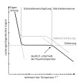 Störstellenerschöpfung.svg 700 × 700; 21 KB
-
 Temperature dependence of material types.svg 1,440 × 720; 33 KB
-
 Tlm article graphics.png 794 × 1,123; 30 KB
-
 Tlm derivation.png 606 × 528; 56 KB
-
 TRANSIÇÃO.gif 194 × 172; 6 KB
-
 USB Tweezers CBP.jpg 171 × 145; 7 KB
-
 Wiki losy elektronu.tif 591 × 657; 1.94 MB
-
 Zlacze m-s.gif 400 × 200; 4 KB
-
 直接遷移1.png 753 × 661; 30 KB
-
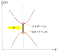
 間接遷移.png 997 × 856; 68 KB
-
 間接遷移1.png 760 × 705; 36 KB


.jpg)


.png)


.jpg)
.jpg)
.jpg)


