Category:Diode diagrams
Jump to navigation
Jump to search
Subcategories
This category has the following 11 subcategories, out of 11 total.
C
D
- DIAC diagrams (21 F)
P
S
- Schottky diode diagrams (10 F)
T
- Tunnel diode diagrams (20 F)
V
- Vacuum diode diagrams (37 F)
Z
- Zener diode diagrams (40 F)
Media in category "Diode diagrams"
The following 146 files are in this category, out of 146 total.
-
 AC current through a diode.png 467 × 133; 5 KB
-
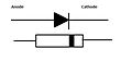 Anode-cathode.jpg 433 × 242; 9 KB
-
 AP-Diode.png 3,580 × 2,458; 163 KB
-
 AusfuerungsformenSchottkyDiode-de.svg 638 × 677; 2 KB
-
 AusfuerungsformenSchottkyDiode-ru.svg 638 × 677; 3 KB
-
 AusfuerungsformenSchottkyDiode.png 556 × 564; 16 KB
-
 Axial diode assembly.png 745 × 818; 54 KB
-
 BackEMFWaveform.png 800 × 594; 249 KB
-
 Backward diode characteristics.svg 270 × 270; 6 KB
-
 Backwarddiode.jpg 500 × 400; 12 KB
-
 Base clipper jp.svg 760 × 200; 27 KB
-
 Bias to n.jpg 463 × 242; 10 KB
-
 Cadmium Teluride photocell.JPG 541 × 431; 16 KB
-
 Carac diode idéale et réelle.svg 1,290 × 1,300; 247 KB
-
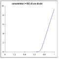 Caractéristique d'une diode.png 400 × 400; 2 KB
-
 Caractéristique idéale.png 2,245 × 1,059; 46 KB
-
 Courbe diode OA85.JPG 1,820 × 2,939; 327 KB
-
 Detektornii diod shotki.jpg 396 × 303; 11 KB
-
 Detektornii diod shotki.svg 656 × 397; 807 bytes
-
 Diod gunn-ru.svg 723 × 861; 1 KB
-
 Diod gunn.jpg 669 × 800; 47 KB
-
 DIODA.png 601 × 511; 37 KB
-
 Diode - ghosting.png 208 × 217; 1,019 bytes
-
 Diode approximation of Voltage vs Current.jpg 950 × 536; 77 KB
-
 Diode char.svg 738 × 720; 8 KB
-
 Diode corba caracteristica (Sockley).png 265 × 270; 2 KB
-
 Diode i-v.jpg 540 × 310; 24 KB
-
 Diode iv curve 450.jpg 450 × 431; 6 KB
-
 Diode laser - polarisation.jpg 470 × 478; 42 KB
-
 Diode limiter input voltage 1000.jpg 1,000 × 962; 29 KB
-
 Diode Modelling Image10.jpg 400 × 400; 16 KB
-
 Diode Modelling Image11.png 400 × 400; 1 KB
-
 Diode Modelling Image3.jpg 400 × 400; 18 KB
-
 Diode Modelling Image5.png 400 × 400; 646 bytes
-
 Diode Modelling Image6.jpg 268 × 87; 3 KB
-
 Diode Modelling Image8.png 400 × 400; 684 bytes
-
 Diode Modelling Image9.jpg 362 × 101; 4 KB
-
 Diode mosfet fr.png 1,500 × 1,050; 66 KB
-
 Diode mosfet-ru.svg 686 × 457; 11 KB
-
 Diode mosfet.png 1,500 × 1,050; 72 KB
-
 Diode mosfet.svg 480 × 320; 10 KB
-
 Diode OA85.JPG 1,586 × 756; 74 KB
-
 Diode symbol cs.svg 111 × 53; 7 KB
-
 Diode-Equiv-Circuit.svg 512 × 640; 31 KB
-
 Diode-IV-Curve-de.svg 500 × 300; 29 KB
-
 Diode-IV-Curve-ru.svg 762 × 454; 1 KB
-
 Diode-IV-Curve-uk.png 500 × 300; 16 KB
-
 Diode-IV-Curve.jpg 967 × 693; 171 KB
-
 Diode-IV-Curve.svg 500 × 300; 24 KB
-
 Diode-Vollständiges Ersatzschaltbild.gif 686 × 387; 5 KB
-
 Diode3.svg 250 × 150; 42 KB
-
 Diode4.svg 250 × 150; 37 KB
-
 Diode5.svg 250 × 150; 38 KB
-
 Diode6.svg 250 × 150; 36 KB
-
 Diode79.gif 462 × 279; 13 KB
-
 DiodeGenCharacteristics1.jpg 1,376 × 720; 135 KB
-
 DiodeGenCharacteristics2.jpg 1,086 × 604; 77 KB
-
 Dioden-Kennlinie 1N4001 differentiell.svg 350 × 425; 16 KB
-
 Dioden-Kennlinie 1N4001.svg 341 × 389; 14 KB
-
 Dioden-Kennlinien00.svg 1,080 × 873; 13 KB
-
 Diodo - curva característica (Sockley).png 265 × 270; 3 KB
-
 Diodo - Modelos de continua.png 807 × 370; 7 KB
-
 DIODO CURVA.jpg 399 × 356; 33 KB
-
 Diodo graph.svg 850 × 756; 13 KB
-
 Diodo polarizzato.JPG 562 × 328; 16 KB
-
 Diodo.JPG 278 × 393; 13 KB
-
 Diodo1.jpg 720 × 540; 32 KB
-
 Diodo2.jpg 720 × 540; 29 KB
-
 Diodo3.jpg 720 × 540; 34 KB
-
 Diòde - Diòde ideau.png 1,218 × 1,077; 92 KB
-
 Diòde - Diòde reau.png 1,063 × 687; 47 KB
-
 Ejercicio.1.b.png 594 × 634; 46 KB
-
 Electrionics Analogy - Valve (Diodes comparison).svg 400 × 300; 106 KB
-
 Elektrolumineszenz.png 807 × 2,471; 106 KB
-
 Epitaxial-planar.svg 500 × 250; 12 KB
-
 Estructura diodo 2.JPG 612 × 434; 40 KB
-
 FET Diode Comparison Chart.JPG 795 × 529; 63 KB
-
 First 3 Resutls.jpg 720 × 540; 72 KB
-
 FlybackWaveform.gif 800 × 598; 266 KB
-
 Forward and Reverse Characteristics for diodes-en.svg 519 × 333; 607 KB
-
 Forward-biased nanofluidic diode.png 529 × 271; 13 KB
-
 GaAlAs U-T.png 450 × 320; 6 KB
-
 Giunzione p–n vs. diodo ideale.png 532 × 335; 2 KB
-
 Hrotova dioda.svg 588 × 600; 5 KB
-
 I-U-Charakteristik p-n-Uebergang Durchbruch.png 821 × 796; 12 KB
-
 I-U-Charakteristik p-n-Uebergang Durchbruch.svg 738 × 720; 6 KB
-
 IV CV of HBVmellan.png 414 × 306; 22 KB
-
 KennlinieDiode resized.jpg 480 × 360; 22 KB
-
 KennlinieIdealeDiode00.svg 747 × 576; 6 KB
-
 Lambda-diode-kennlinie.svg 490 × 470; 6 KB
-
 LambdaDiode.png 400 × 769; 5 KB
-
 Ledwhitecharcurp.png 538 × 490; 5 KB
-
 Lidhje e shkurt.png 415 × 126; 6 KB
-
 Magnetdiode-de.svg 464 × 478; 1 KB
-
 Magnetdiode-ru.svg 464 × 478; 1 KB
-
 Model VD.svg 164 × 179; 43 KB
-
 Peak clipper jp.svg 760 × 200; 29 KB
-
 PIN dioda.png 490 × 352; 15 KB
-
 Pin-Diode.svg 372 × 85; 8 KB
-
 PIN2.png 698 × 892; 43 KB
-
 Pn diode band diagram sketch.png 200 × 160; 2 KB
-
 PN diode with electrical symbol-ru.svg 737 × 330; 2 KB
-
 PN diode with electrical symbol-tr.svg 328 × 110; 10 KB
-
 Pn Junction IV Characteristic.svg 400 × 400; 17 KB
-
 PN-diode med elektrisk symbol.svg 328 × 110; 11 KB
-
 Pn-Diode-Aufbau.svg 275 × 373; 8 KB
-
 Poster-Diode.png 2,170 × 3,072; 1.49 MB
-
 Process of the barrier capacitance.svg 319 × 159; 13 KB
-
 Punto di lavoro del diodo.PNG 378 × 349; 5 KB
-
 Qarku i hapur.png 411 × 121; 7 KB
-
 RadarDiode.jpg 113 × 85; 3 KB
-
 Recuperacio inversa del diodo.JPG 345 × 233; 20 KB
-
 Relay animation with flyback diode.gif 2,099 × 824; 295 KB
-
 Schem znacka diody.png 372 × 199; 5 KB
-
 Schema.diodo.a.giunzione.png 202 × 179; 28 KB
-
 Schottky-Diode-Aufbau.svg 512 × 694; 8 KB
-
 Schéma zapojení PIN diody s předpětím.png 632 × 293; 8 KB
-
 SE Diode Construction.svg 421 × 125; 7 KB
-
 Semiconductor - Esquèma simplificat d'una joncion P-N.png 4,241 × 2,176; 1.13 MB
-
 SiC Rectifiers V01.png 1,479 × 436; 42 KB
-
 Simbol diod.JPG 433 × 207; 8 KB
-
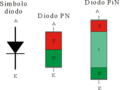 Simbolo diodo e struttura diodoPN e diodo PiN.png 400 × 300; 3 KB
-
 SLED LD.svg 425 × 425; 21 KB
-
 SPAD Cross-section.gif 640 × 341; 15 KB
-
 Spectral ripple of SLED.svg 368 × 317; 11 KB
-
 Spitzendiode germanium.gif 580 × 158; 8 KB
-
 SRL 3D.png 3,402 × 2,322; 221 KB
-
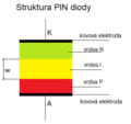 Struktura PIN diody.png 736 × 696; 12 KB
-
 Tektronix 571 Semiconductor Curve Plotter.jpg 1,935 × 1,126; 567 KB
-
 TiepeseDiodeSpanningsStroomKurve.svg 400 × 400; 7 KB
-
 Transfer function of an improved super diode.svg 623 × 511; 6 KB
-
 Two diode structures.png 488 × 451; 18 KB
-
 V-A Character Si Ge diod.png 733 × 682; 119 KB
-
 V-A Characteristic diod.svg 619 × 515; 32 KB
-
 V-a characteristic diodes si ge-ru.svg 744 × 514; 837 bytes
-
 V-a characteristic diodes si ge.svg 260 × 180; 8 KB
-
 V-a characteristic diodes.svg 260 × 180; 12 KB
-
 V-a characteristic LED.svg 230 × 190; 7 KB
-
 Varicap characteristics.svg 240 × 200; 13 KB
-
 VFH varikap.svg 726 × 560; 5 KB
-
 Zener grafik.jpg 225 × 153; 2 KB
-
 Вольт-амперная характеристика полупроводникового диода.png 3,107 × 2,330; 112 KB
-
 Коэффициент лавинного размножения в Si от Т.svg 722 × 625; 21 KB
-
 Плавка pn-перехода по Олу.PNG 852 × 799; 69 KB
-
 صمام ثنائي.png 404 × 105; 2 KB
-
 ಅರೆವಹಕ.png 1,200 × 402; 22 KB


.png)


.png)


.svg)


