Category:BJT diagrams
Jump to navigation
Jump to search
BJT = Bipolar junction transistors
Subcategories
This category has the following 5 subcategories, out of 5 total.
Media in category "BJT diagrams"
The following 111 files are in this category, out of 111 total.
-
 2SC1815 Amp-linearity-sample1.png 438 × 310; 7 KB
-
 2SC1815 Ic-Vbe-sample1.png 447 × 310; 6 KB
-
-
 Betragsfrequenzgänge für Bipolartransistor.svg 478 × 425; 14 KB
-
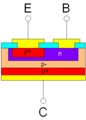
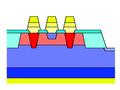
 Bipolar Junction Transistor NPN Structure integrated vertical.png 1,055 × 362; 17 KB
-
 Bipolar Junction Transistor NPN Structure.png 322 × 450; 8 KB
-
 Bipolar Junction Transistor NPN Structure.svg 317 × 427; 8 KB
-
 Bipolar Junction Transistor PNP Structure integrated lateral.png 1,076 × 391; 18 KB
-
 Bipolar Junction Transistor PNP Structure.png 323 × 450; 8 KB
-
 Bipolar transistor-undescribed.png 800 × 600; 4 KB
-
 Bipolar transistor.png 800 × 600; 20 KB
-
 Bipolar transistor.svg 985 × 658; 25 KB
-
 Bipolare npn-Leistungstransistor Schema (DE).svg 425 × 355; 21 KB
-
 Bipolarepiplanar junction transistor.svg 315 × 350; 13 KB
-
 Bipolartransistor1.PNG 567 × 365; 5 KB
-
 Bipolartransistor1.svg 567 × 365; 34 KB
-
 Bipolartransistor2.PNG 567 × 387; 6 KB
-
 Bipolartransistor3.PNG 567 × 387; 6 KB
-
 BJT Teminal Identificaion (Measurement)-ar.svg 520 × 210; 57 KB
-
 BJT Teminal Identificaion (Measurement)-en.svg 520 × 210; 81 KB
-
 BJT Teminal Identificaion-ar.svg 1,100 × 350; 110 KB
-
 BJT Teminal Identificaion-en.svg 1,100 × 350; 117 KB
-
 BJT-transistor01.png 500 × 300; 14 KB
-
 Bulk Resistors in Bipolar-Transistor.svg 177 × 213; 18 KB
-
 CaractTransistorBip2.png 227 × 250; 2 KB
-
 Current-Voltage relationship of BJT zh.png 976 × 589; 44 KB
-
 Current-Voltage relationship of BJT.png 981 × 590; 42 KB
-
 Diak PNP.PNG 315 × 624; 8 KB
-
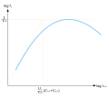
 Early effect (graph - I C vs V CE).svg 300 × 125; 25 KB
-
 Early effect (IC-VCE) zh-hans.svg 800 × 400; 16 KB
-
 Early effect (IC-VCE) zh-hant.svg 800 × 400; 17 KB
-
 Early effect.png 739 × 304; 23 KB
-
 Experimenting with a "Slayer oscillator" I.jpg 320 × 234; 31 KB
-
 Graded hetero bipolar transistor.png 398 × 338; 14 KB
-
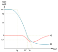
 Gummel-Plot Early- und Hochstromeffekt.svg 206 × 252; 17 KB
-
 Gummel-Poon1.png 1,876 × 1,496; 87 KB
-
 H ie.svg 240 × 180; 48 KB
-
 ICB0 leakage transistor-ar.svg 346 × 151; 64 KB
-
 ICB0 leakage transistor-en.svg 346 × 151; 74 KB
-
 ICE0 leakage transistor-ar.svg 346 × 156; 58 KB
-
 ICE0 leakage transistor-en.svg 346 × 156; 74 KB
-
 NPN Band Diagram Active-ar.svg 400 × 219; 92 KB
-
 NPN Band Diagram Active.svg 375 × 205; 30 KB
-
 NPN Band Diagram Equilibrium-ar.svg 427 × 245; 65 KB
-
 NPN Band Diagram Equilibrium.svg 400 × 230; 13 KB
-
 NPN BJT (Planar) Cross-section.svg 300 × 175; 9 KB
-
 NPN BJT ar.svg 475 × 200; 84 KB
-
 NPN BJT Basic Operation (Active) ar.svg 475 × 225; 32 KB
-
 NPN BJT Basic Operation (Active) DE.svg 475 × 225; 27 KB
-
 NPN BJT Basic Operation (Active) fr.svg 475 × 225; 32 KB
-
 NPN BJT Basic Operation (Active).svg 475 × 225; 32 KB
-
 Npn BJT cross section.PNG 455 × 188; 8 KB
-
 Npn bjt cross section.svg 470 × 203; 7 KB
-
 NPN BJT Minority Carrier Profiles (Active mode).svg 475 × 300; 25 KB
-
 NPN BJT.svg 475 × 200; 13 KB
-
 NPN charge carrier movments-ar.svg 346 × 271; 394 KB
-
 NPN charge carrier movments-en.svg 346 × 271; 424 KB
-
 NPN common emitter configuration.svg 384 × 240; 25 KB
-
 NPN common-base configuration.svg 384 × 240; 23 KB
-
 NPN common-base flow -en.svg 384 × 240; 38 KB
-
 NPN common-collector configuration.svg 384 × 240; 25 KB
-
 NPN Currents-ar.svg 346 × 151; 125 KB
-
 NPN Currents-en.svg 346 × 151; 133 KB
-
 Npn diode circuit diagram.gif 499 × 248; 9 KB
-
 Npn heterostructure bands.svg 428 × 271; 7 KB
-
 NPN transistor as diode.png 1,589 × 1,701; 749 KB
-
 NPN transistor basic operation english.svg 461 × 262; 15 KB
-
 NPN transistor basic operation ml.svg 491 × 280; 15 KB
-
 NPN transistor basic operation pa.svg 461 × 262; 15 KB
-
 NPN transistor basic operation pl.png 2,000 × 1,137; 80 KB
-
 NPN transistor basic operation Portugues.png 460 × 262; 17 KB
-
 NPN transistor basic operation-bn.svg 461 × 262; 15 KB
-
 NPN transistor basic operation-kn.svg 461 × 262; 18 KB
-
 NPN transistor basic operation-ta.svg 461 × 262; 13 KB
-
 NPN transistor basic operation-te.svg 461 × 262; 14 KB
-
 NPN transistor basic operation.svg 461 × 262; 16 KB
-
 Npn-structure.png 390 × 334; 3 KB
-
 Pnp Base Narrowing.png 528 × 474; 12 KB
-
 Pnp base narrowing.svg 507 × 432; 15 KB
-
 PNP BJT-ar.svg 507 × 213; 81 KB
-
 PNP BJT.svg 475 × 200; 13 KB
-
 PNP charge carrier movments-ar.svg 346 × 271; 415 KB
-
 PNP charge carrier movments-en.svg 346 × 271; 430 KB
-
 PNP common base configuration.svg 384 × 240; 23 KB
-
 PNP common emitter configuration.svg 384 × 240; 25 KB
-
 PNP common-base flow -en.svg 384 × 240; 34 KB
-
 PNP common-collector configuration.svg 384 × 240; 25 KB
-
 Pnp currents-ar.svg 346 × 146; 128 KB
-
 Pnp currents-en.svg 346 × 146; 139 KB
-
 Pnp Heterostructure Bands.png 426 × 288; 24 KB
-
 Pnp-structure.png 390 × 334; 4 KB
-
 Regioni transistore BJT ad emettitore comune.png 484 × 285; 2 KB
-
 Scheme of bipolar junction transistor de.png 790 × 450; 18 KB
-
 SiGe HBT Gummel Plot.png 1,343 × 732; 83 KB
-
 Stromverstärkung vs Kollektorstrom.svg 397 × 209; 23 KB
-
 Transistor animation.gif 640 × 480; 24 KB
-
 Transistor Ausgangskennlinienfeld.svg 390 × 234; 23 KB
-
 Transistor BJT puissance.png 500 × 452; 282 KB
-
 Transistor description en.svg 300 × 400; 35 KB
-
 Transistor description ja.png 300 × 400; 27 KB
-
 Transistor description ja.svg 300 × 400; 36 KB
-
 Transistor description template.xcf 300 × 400; 31 KB
-
 Transistor description zh.svg 300 × 400; 35 KB
-
 Transistor Silicon Diagram NPN.png 300 × 174; 2 KB
-
 Transistor Simple Circuit Diagram with NPN Labels.svg 720 × 720; 7 KB
-
 Transistor-Arbeitsbereich.png 300 × 300; 32 KB
-
 Tranzystor npn.svg 600 × 250; 8 KB
-
 Tranzystor pnp.svg 600 × 250; 8 KB
-
 Verlauf der Transitzeit eines Bipolartransistors.svg 478 × 283; 22 KB
-
 Verstärkungskennlinie BC547B.svg 820 × 779; 14 KB
-
 Структура NPN транзистора и его токи.svg 354 × 230; 2 KB


.svg)
_zh-hans.svg)
_zh-hant.svg)


_Cross-section.svg)

_ar.svg)
_DE.svg)
_fr.svg)
.svg)


.svg)


.svg)
-ar.svg)
-en.svg)