Category:Images from WikiAppunti
Jump to navigation
Jump to search
Pages in category "Images from WikiAppunti"
The following 2 pages are in this category, out of 2 total.
Media in category "Images from WikiAppunti"
The following 200 files are in this category, out of 486 total.
(previous page) (next page)-
 1-persistent CSMA⁄CD collision.png 208 × 228; 2 KB
-
 1st-order system impulse response.png 388 × 260; 2 KB
-
 1st-order system step response.png 484 × 291; 3 KB
-
 2-bit parallel flash AD converter thermometric scale.png 182 × 243; 1 KB
-
 2nd-order system step response 1.png 198 × 221; 1 KB
-
 2nd-order system step response 2.png 189 × 119; 928 bytes
-
 2nd-order system step response 3.png 203 × 167; 1 KB
-
 2nd-order system step response 4.png 190 × 125; 976 bytes
-
 2nd-order system step response 5-6 - Max overshoot typ values.png 138 × 146; 618 bytes
-
 2nd-order system step response 5.png 260 × 189; 1 KB
-
 2nd-order system step response 6.png 217 × 154; 1 KB
-
 2nd-order system step response 7.png 218 × 155; 986 bytes
-
 3-dB bandwidth definition (linear).png 225 × 225; 1 KB
-
 3-dB bandwidth definition (logarithmic).png 225 × 225; 1 KB
-
 ABC letters white icon.svg 700 × 700; 6 KB
-
 Active differentiator.png 450 × 239; 2 KB
-
 Active integrator.png 450 × 243; 2 KB
-
 Active ring topology.png 440 × 428; 66 KB
-
 Adder shift block diagram interconnection (in function of s).png 804 × 187; 3 KB
-
 Address learning e frame forwarding.png 780 × 390; 6 KB
-
 Agenda white icon.svg 600 × 600; 122 KB
-
 Albero delle decisioni.png 669 × 328; 6 KB
-
 Amplifier block diagram fundamental block.png 413 × 118; 1 KB
-
 Amplifier with high-pass RC cell frequency analysis.png 399 × 281; 4 KB
-
 Amplifier with high-pass RC cell.png 381 × 265; 5 KB
-
 Amplifier with low-pass RC cell.png 656 × 307; 8 KB
-
 Analogue anticipatory or attenuating compensation network.png 254 × 202; 1 KB
-
 Analogue D-type compensator.png 281 × 154; 958 bytes
-
 Analogue I-type compensator.png 254 × 149; 806 bytes
-
 Analogue integral-derivative compensation network.png 298 × 202; 1 KB
-
 Analogue P-type compensator.png 254 × 154; 871 bytes
-
 Analogue PD-type compensator.png 254 × 176; 1 KB
-
 Analogue PI-type compensator.png 254 × 153; 934 bytes
-
 Analogue PID-type compensator.png 254 × 176; 1 KB
-
 Anticipatory compensation network Bode plots.png 521 × 355; 4 KB
-
 Apertura connessione TCP.png 800 × 446; 24 KB
-
 Arbitraggio bus centralizzato con polling.png 766 × 216; 21 KB
-
 ASK modulation.png 348 × 115; 1 KB
-
 Asymptotically stable equilibrium state example.png 366 × 235; 2 KB
-
 Asymptotically stable nominal movement example.png 308 × 271; 3 KB
-
 ATM PDU format.png 869 × 416; 4 KB
-
 Attenuating compensation network Bode plots.png 358 × 367; 3 KB
-
 Attraversamento albero binario.png 278 × 238; 3 KB
-
 Background green icon.png 1,250 × 1,250; 11 KB
-
 Backward difference method.png 381 × 288; 6 KB
-
 Balloons white icon.svg 700 × 700; 5 KB
-
 Band-pass amplifier with RC cells.png 681 × 283; 4 KB
-
 Bilinear transformation.png 382 × 287; 6 KB
-
 Bit stuffing.png 396 × 103; 1 KB
-
 BJT transistor in use on switching.png 130 × 220; 874 bytes
-
 BJT-transistor low-side switch.png 644 × 325; 3 KB
-
 Bus connection with transceiver.png 367 × 188; 2 KB
-
 Bus multiplexato.png 316 × 93; 1 KB
-
 Bus parallelo.png 376 × 138; 2 KB
-
 Bust transfer.png 412 × 149; 2 KB
-
 Butterworth filter energy spectrum.png 207 × 195; 1,019 bytes
-
 Bypass capacitors.png 325 × 180; 1 KB
-
 Cella RAM dinamica.png 297 × 158; 1 KB
-
 Cella RAM statica.png 410 × 238; 2 KB
-
 Cella ROM.png 297 × 158; 1 KB
-
 Characteristic of a H-state CMOS inverter.png 310 × 234; 2 KB
-
 Characteristic of a L-state CMOS inverter.png 239 × 204; 1 KB
-
 Charge density and electric field of a capacitor.png 540 × 237; 2 KB
-
 Chiusura connessione TCP.png 243 × 270; 2 KB
-
 Circuito con clock jitter e ritardi di propagazione.png 411 × 264; 2 KB
-
 Circuito con clock jitter.png 369 × 263; 2 KB
-
 Circuito lettura sincrona.png 296 × 164; 2 KB
-
 Circuito scrittura asincrona.png 356 × 181; 2 KB
-
 Circuito scrittura semisincrona.png 365 × 178; 2 KB
-
 Circuito scrittura sincrona.png 298 × 164; 2 KB
-

-

-
 Classi di indirizzi IPv4.png 535 × 368; 4 KB
-
 Classificazione movimenti nominali per stabilità interna.png 548 × 95; 2 KB
-
 Closed-loop control system block diagram with disturbances.png 503 × 190; 2 KB
-

-
 CMOS inverter with 3S output.png 323 × 183; 1 KB
-
 CMOS inverter with TP output.png 217 × 172; 945 bytes
-
 CMOS inverter.png 317 × 261; 1 KB
-
 CMOS transition times.png 432 × 147; 824 bytes
-
 Collegamento CMOS a bus con uscite 3S.png 164 × 264; 1 KB
-
 Collision detection reti LAN.png 643 × 322; 3 KB
-
 Common and differential modes in an amplifier.png 535 × 398; 3 KB
-
 Compatibilità tra porte logiche.png 338 × 381; 2 KB
-
 Complex poles Bode plot (module).png 309 × 212; 2 KB
-
 Complex poles Bode plot (phase).png 305 × 189; 1 KB
-
 Confronto filtro passa-basso ideale e reale.png 511 × 151; 1 KB
-
 Conjugate complex number representation.png 237 × 178; 732 bytes
-
 Connection CMOSes to bus through OC outputs.png 151 × 237; 900 bytes
-
 Constant Bode plot (module).png 228 × 150; 617 bytes
-
 Constant Bode plot (phase).png 204 × 163; 609 bytes
-
 Constant signal decomposition.png 872 × 255; 4 KB
-
 Contributi portatori maggioritari giunzione p–n.png 556 × 243; 3 KB
-
 Contributions green icon.png 1,250 × 1,250; 209 KB
-
 Convergenza modi naturali LTI TC.png 363 × 306; 4 KB
-
 Convergenza modi naturali LTI TD.png 363 × 307; 5 KB
-
 Counting sort.png 724 × 238; 6 KB
-
 Critic behaviour of comparator without hysteresis.png 403 × 160; 1 KB
-
 Criticità algoritmo di backward learning.png 1,210 × 419; 12 KB
-
 Crosstalk between conductors.png 256 × 174; 1 KB
-
 Crosstalk due to capacitive couplings 1.png 144 × 340; 1 KB
-
 Crosstalk due to capacitive couplings 2.png 256 × 289; 2 KB
-
 CSMA collision synchronization.png 385 × 445; 5 KB
-
 Current follower.png 447 × 257; 2 KB
-
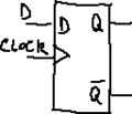
 D latch flip-flop circuit.png 311 × 178; 1 KB
-
 D latch flip-flop functional symbol.png 111 × 110; 466 bytes
-
 D master-slave flip-flop circuit.png 423 × 205; 2 KB
-
 D master-slave flip-flop functional symbol.png 128 × 110; 528 bytes
-
 D-flip-flop synchronous counter circuit.png 647 × 156; 2 KB
-
 Delayer block diagram fundamental block.png 442 × 51; 932 bytes
-
 Dependence between open-loop and closed-loop function.png 266 × 232; 1 KB
-

-
 Derivative monostable circuit.png 339 × 137; 1 KB
-
 Derivative monostable graphs.png 221 × 429; 2 KB
-
 Descrizione probabilistica processo casuale.png 1,051 × 484; 10 KB
-
 DFT circular shift.png 489 × 358; 3 KB
-
 DFT interpretation.png 237 × 177; 1 KB
-
 Diagramma a occhio.png 384 × 294; 3 KB
-
 Diagramma di flusso CSMA 0-persistente.png 413 × 510; 4 KB
-
 Diagramma di flusso CSMA 1-persistente.png 413 × 510; 3 KB
-
 Diagramma di flusso Slotted ALOHA.png 333 × 379; 2 KB
-
 Diagramma spazio-temporale commutazione di circuito.png 622 × 665; 7 KB
-
 Diagramma spazio-temporale commutazione di pacchetto.png 540 × 603; 6 KB
-
 Diagramma stati.png 426 × 252; 3 KB
-
 Diagramma temporale lettura asincrona.png 424 × 410; 3 KB
-
 Diagramma temporale lettura sincrona.png 414 × 392; 3 KB
-
 Diagramma temporale scrittura asincrona.png 479 × 476; 5 KB
-
 Diagramma temporale scrittura sincrona.png 307 × 335; 3 KB
-
 Differential amplifier with non-ideal generators.png 513 × 249; 2 KB
-
 Differential amplifier.png 311 × 202; 1 KB
-
 Digital control system basic diagram.png 798 × 174; 4 KB
-
 Digital signal as random process.png 385 × 180; 1 KB
-
 Discrete-time absolute bandwidth definition.png 453 × 235; 2 KB
-
 Discrete-time equivalent bandwidth definition.png 225 × 199; 1 KB
-
 Discrete-time percentage bandwidth definition.png 245 × 206; 2 KB
-
 Distributed-parameter interconnect model.png 598 × 119; 2 KB
-
 DIT N4.png 433 × 229; 3 KB
-
 Divisione di codice.png 525 × 282; 4 KB
-
 DMA controller.png 535 × 214; 2 KB
-
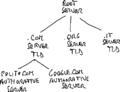 DNS hierarchy.png 460 × 351; 3 KB
-
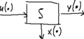 Dynamic system.png 248 × 116; 748 bytes
-
 Effects of skew on setup times.png 249 × 234; 1 KB
-
 Emoticon white icon.svg 700 × 700; 3 KB
-
 Enhanced PID regulator.png 541 × 280; 3 KB
-
 Equivalent circuit for Zener diode.png 633 × 192; 2 KB
-
 Equivalent noise bandwidth definition.png 225 × 199; 1 KB
-
 Errore dimensionamento finestre selective repeat.png 735 × 797; 11 KB
-
 Esempio di arbitraggio del bus.png 228 × 307; 2 KB
-
 Esempio di circuiti a più ingressi.png 390 × 259; 2 KB
-
 Esempio di LAN estesa.png 728 × 239; 5 KB
-
 Esempio ICMP Redirect.png 395 × 343; 4 KB
-
 Esempio interconnessione hub.png 638 × 447; 5 KB
-
 Esempio netmask IPv4.png 758 × 89; 2 KB
-
 Esempio prestazioni topologia.png 668 × 650; 23 KB
-
 Esempio Slotted ALOHA.png 623 × 198; 3 KB
-
 Esempio tabella di routing.png 1,725 × 470; 17 KB
-
 Evenly-distributed signal sequence.png 552 × 216; 2 KB
-
 Exclamation mark white icon.svg 600 × 600; 957 bytes
-
 Fasi di fetch in UC cablata.png 274 × 561; 3 KB
-
 FCFS bus arbitration.png 267 × 237; 2 KB
-
 Feedback block diagram interconnection (discrete-time).png 368 × 187; 1 KB
-
 Feedback block diagram interconnection (in function of s).png 381 × 186; 2 KB
-
 Feedback block diagram interconnection.png 417 × 194; 2 KB
-
 Feedback system model.png 362 × 180; 1 KB
-
 Fibonacci.png 746 × 309; 7 KB
-
 Filter analogue vs. discrete frequency.png 242 × 201; 1 KB
-
 Filtro di tenuta costante a tratti sample e hold.png 326 × 169; 1 KB
-
 Finestra di congestione TCP.png 352 × 223; 2 KB
-
 Finestra di ricezione selective repeat.png 453 × 156; 2 KB
-
 Finestra di trasmissione selective repeat.png 530 × 200; 3 KB
-
 Finestre di lavoro fibre ottiche.png 528 × 320; 2 KB
-
 Flip-flop anti-rebound system circuit.png 589 × 171; 2 KB
-
 Flip-flop SR sincrono.png 397 × 221; 2 KB
-
 Flip-flop SR.png 297 × 148; 1,008 bytes
-
 Forma prefissa.png 267 × 126; 1 KB
-
 Formato campo di controllo PDU HDLC.png 1,320 × 336; 9 KB
-
 Formato PDU CS.png 598 × 302; 3 KB
-
 Formato PDU Ethernet vs. IEEE 802.3.png 1,028 × 525; 11 KB
-
 Formato PDU HDLC.png 686 × 165; 3 KB
-
 Formato PDU LLC.png 673 × 204; 3 KB
-
 Formato PDU PPP.png 818 × 162; 4 KB
-
 Formato PDU SNAP.png 953 × 204; 4 KB
-
 Forward difference method.png 381 × 288; 6 KB
-
 Frequency memodulation (step 1).png 475 × 162; 1 KB
-
 Frequency modulation (frequency components).png 482 × 465; 5 KB
-
 Full shift-register circuit.png 332 × 243; 2 KB
-
 Funzione porta (tempo e frequenza).png 518 × 185; 2 KB
-
 Gain margin.png 568 × 255; 3 KB
-
 Gate convolution (frequency).png 362 × 297; 2 KB
-
 Gate convolution (triangular case).png 280 × 196; 2 KB
-
 Gate convolution.png 494 × 293; 3 KB
-
 Gate function Fourier transformation.png 362 × 107; 860 bytes
-
 Generalized adder.png 352 × 366; 3 KB
-
 Generic system.png 248 × 74; 589 bytes
-
 Geographical addressing.png 139 × 161; 690 bytes
-
 Gibbs phenomenon example.png 490 × 216; 2 KB
-
 Giunzione p–n vs. diodo ideale.png 532 × 335; 2 KB
-
 Golden open book.png 200 × 200; 22 KB
-
 Gram-Schmidt process (case A, steps 2-3).png 472 × 292; 3 KB
-
 Gram-Schmidt process (case B, step 2-3).png 485 × 245; 2 KB


.png)
.png)


.png)
.png)


.png)
.png)


.png)
.png)


.png)


.png)
.png)


.png)
.png)
.png)
.png)
.png)
.png)