File:Electron density wave - plasmon excitations.png
Jump to navigation
Jump to search
No higher resolution available.
Electron_density_wave_-_plasmon_excitations.png (666 × 199 pixels, file size: 2 KB, MIME type: image/png)
Captions
Captions
Add a one-line explanation of what this file represents

|
This diagram image could be re-created using vector graphics as an SVG file. This has several advantages; see Commons:Media for cleanup for more information. If an SVG form of this image is available, please upload it and afterwards replace this template with
{{vector version available|new image name}}.
It is recommended to name the SVG file “Electron density wave - plasmon excitations.svg”—then the template Vector version available (or Vva) does not need the new image name parameter. |
Summary
[edit]
| Description |
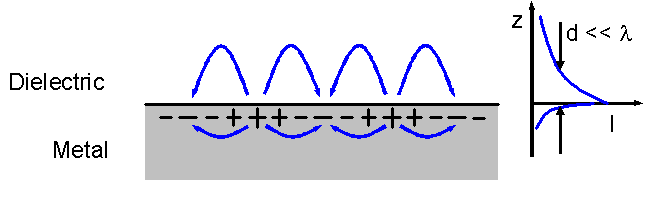
English: Schematic representation of an electron density wave propagating along a metal/dielectric interface. The charge density oscillations and associated electromagnetic fields are called surface plasmon-polariton waves. The exponential dependence of the electromagnetic field intensity on the distance away from the interface is shown on the right. These waves can be excited very efficiently with light in the visible range of the electromagnetic spectrum.
Presently, metallic nanostructures are used to fabricate/analyze:
|
| Date | |
| Source | National Science Foundation - Center for Probing the Nanoscale |
| Author | Center for Probing the Nanoscale - |
| Permission (Reusing this file) |
Public Domain - NSF (of US government) |
Licensing
[edit]
This work is in the public domain in the United States because it is a work prepared by an officer or employee of the United States Government as part of that person’s official duties under the terms of Title 17, Chapter 1, Section 105 of the US Code.
Note: This only applies to original works of the Federal Government and not to the work of any individual U.S. state, territory, commonwealth, county, municipality, or any other subdivision. This template also does not apply to postage stamp designs published by the United States Postal Service since 1978. (See § 313.6(C)(1) of Compendium of U.S. Copyright Office Practices). It also does not apply to certain US coins; see The US Mint Terms of Use.
|
 | |
| This file has been identified as being free of known restrictions under copyright law, including all related and neighboring rights. | ||
File history
Click on a date/time to view the file as it appeared at that time.
| Date/Time | Thumbnail | Dimensions | User | Comment | |
|---|---|---|---|---|---|
| current | 15:41, 1 August 2010 | 666 × 199 (2 KB) | Dbc334 (talk | contribs) | == {{int:filedesc}} == {{Information |Description={{en|1=[http://www.stanford.edu/group/cpn/research/investigators_2.html Schematic representation] of an electron density wave propagating along a metal/dielectric interface. The charge density oscillations |
You cannot overwrite this file.
File usage on Commons
The following page uses this file:
File usage on other wikis
The following other wikis use this file:
- Usage on ar.wikipedia.org
- Usage on ca.wikipedia.org
- Usage on en.wikipedia.org
- Usage on es.wikipedia.org
- Usage on fr.wikipedia.org
- Usage on ja.wikipedia.org
- Usage on zh.wikipedia.org